Industrial-grade precision instruments certified for laboratory, defense, aerospace, and critical infrastructure testing.
In the modern landscape of high-precision scientific analysis, the capability to capture accurate, non-contact thermal information is critical. Hubei Sema Image Co., Ltd. stands as a premier global developer and manufacturer specializing in the infrared and thermal imaging industry. Built upon a foundation of independent intellectual property rights, our comprehensive portfolio delivers unprecedented accuracy, stability, and spatial resolution.
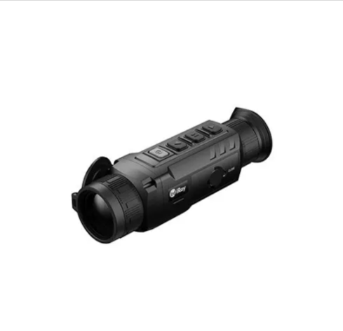
By designing and fabricating proprietary infrared detectors, thermal camera cores, and integrated modules, we cater directly to demanding terminal applications. Our flagship systems—including highly specialized Thermal Imaging Cameras—serve crucial functions across security, industrial monitoring, automotive, healthcare, and laboratory environments. Today, our field-proven solutions are deployed in over 90 countries, offering academic, industrial, and defense researchers exceptional diagnostic clarity.
With a massive talent pool exceeding 1,200 dedicated professionals—nearly 50% of whom operate directly within our R&D divisions—we systematically push the limits of optoelectronic engineering. Our patent portfolio includes more than 700 registered intellectual properties, representing breakthroughs in MEMS sensor design, advanced IC architectures, and software algorithms. Key innovations like the Matrix III image enhancement framework and AI-Temp intelligence ensure that our products remain at the frontier of precision science.
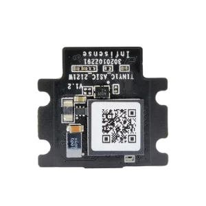
Understanding the core electronic and algorithmic architectures that differentiate professional laboratory thermography instruments from consumer-grade sensors.
Our proprietary algorithm mitigates temporal and spatial noise in microbolometer sensors. By processing pixel arrays dynamically, Matrix III delivers highly defined structural boundaries and high thermal sensitivity (NETD <30mK to 50mK).
Laboratory measurement requires absolute reliability. AI-Temp algorithms compensate for changing ambient environments, preventing drift in measurements and maintaining precision within ±2°C or ±2% across wide target ranges.
Non-Uniformity Correction (NUC) is essential for consistent thermal performance. Our intelligent automated shutter calibration mechanism ensures that the sensor responds uniformly across all pixels, removing spatial anomalies dynamically.
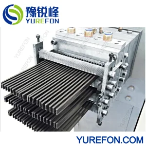
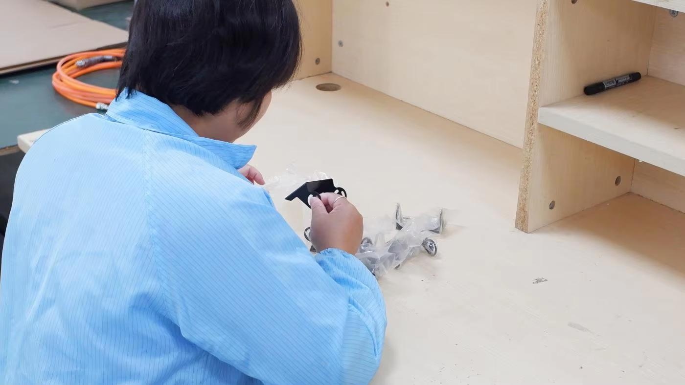
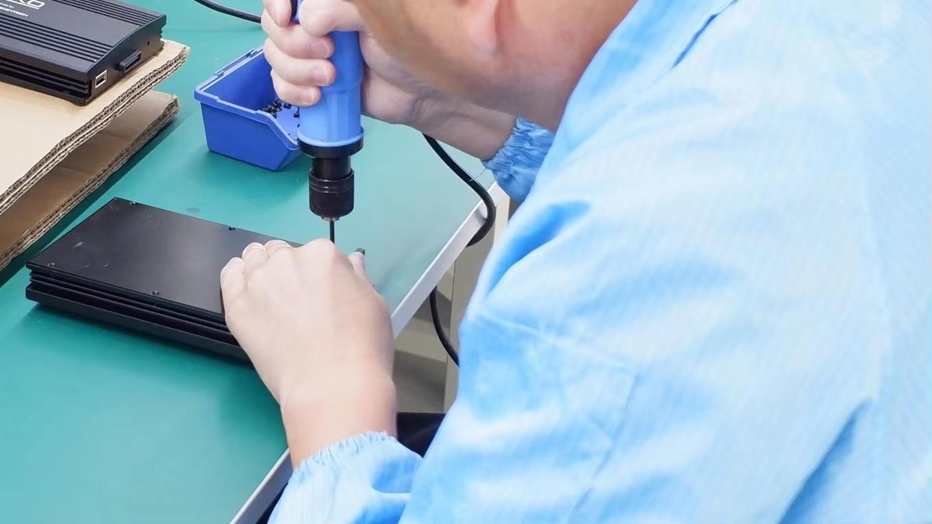
From raw silicon wafers to hermetically sealed optical structures, take an detailed look at our internal manufacturing workflow.
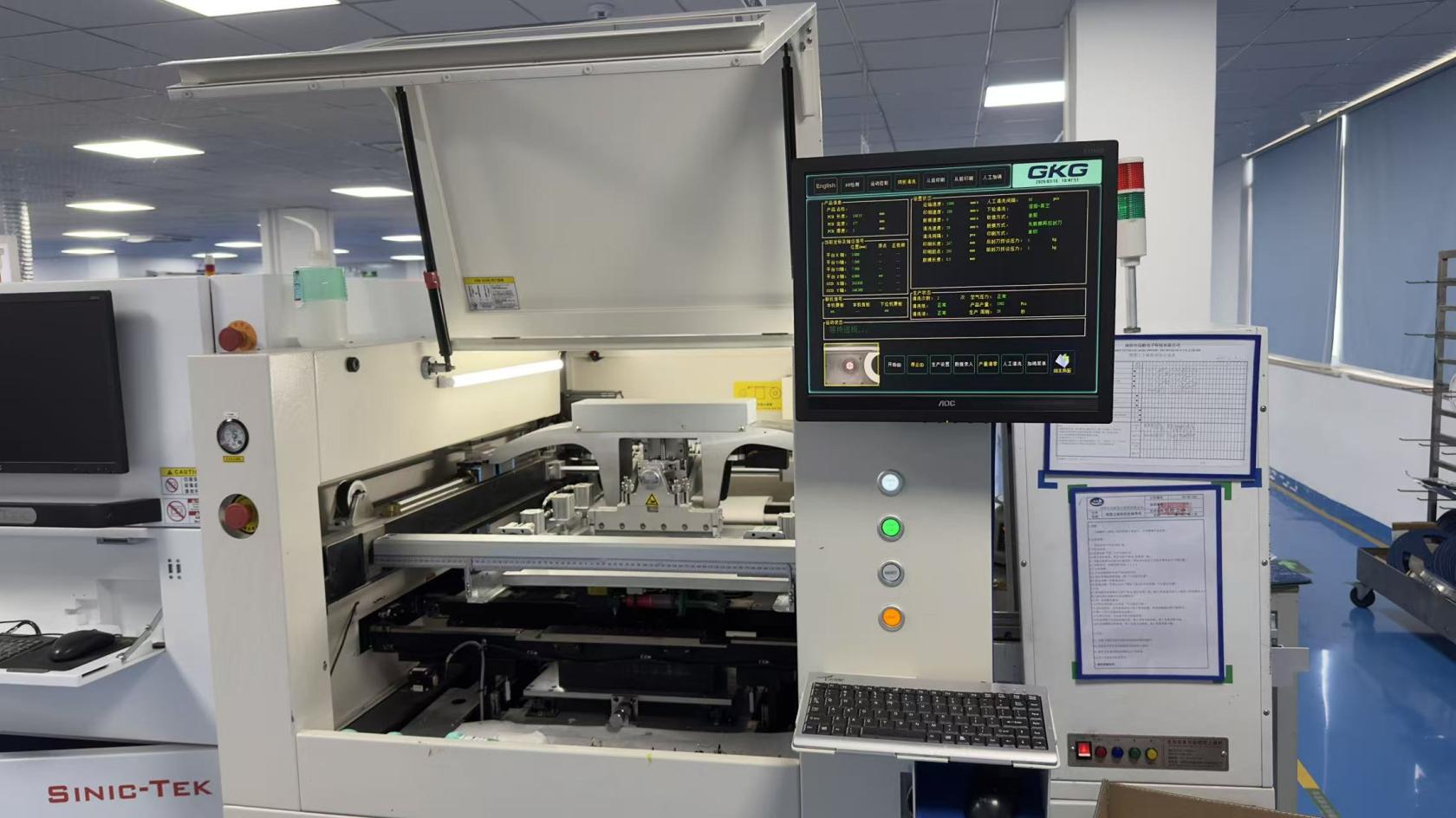
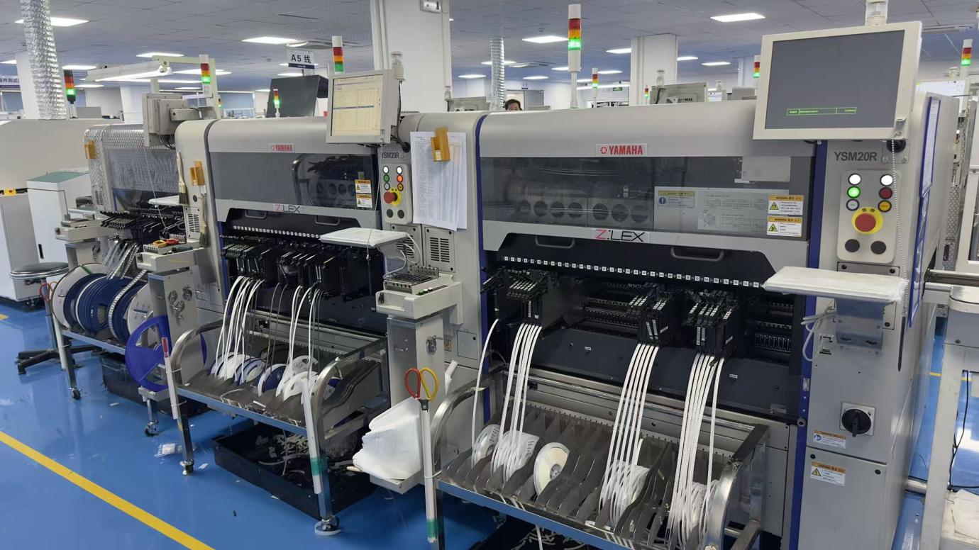
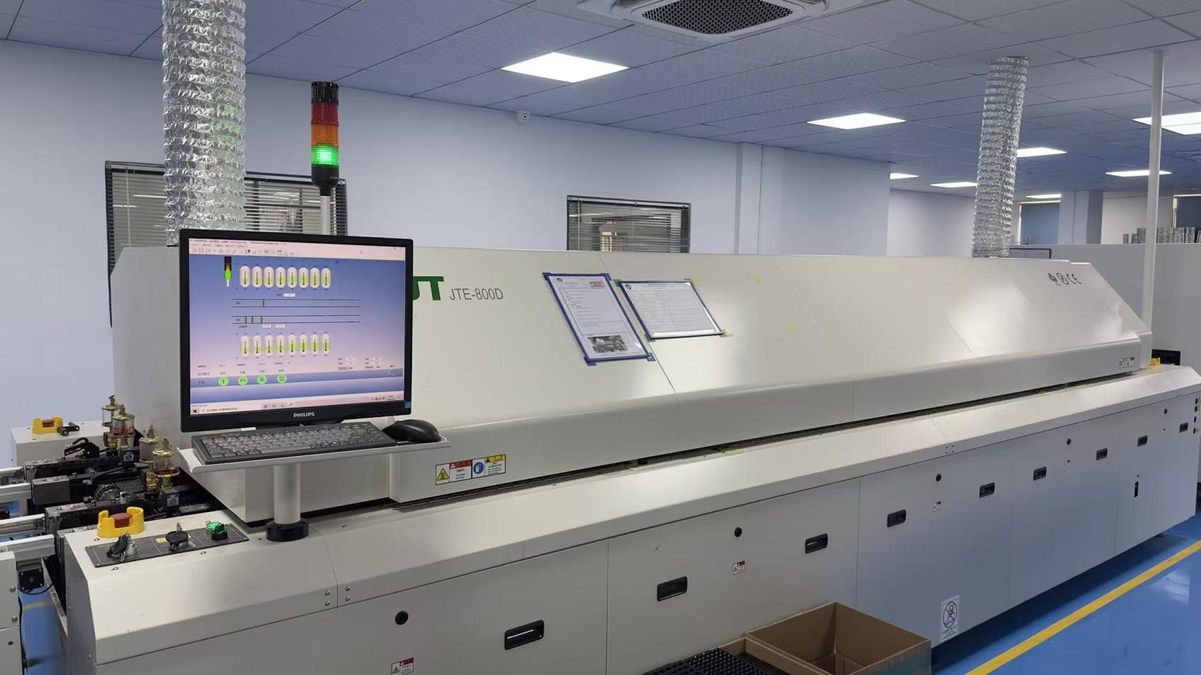
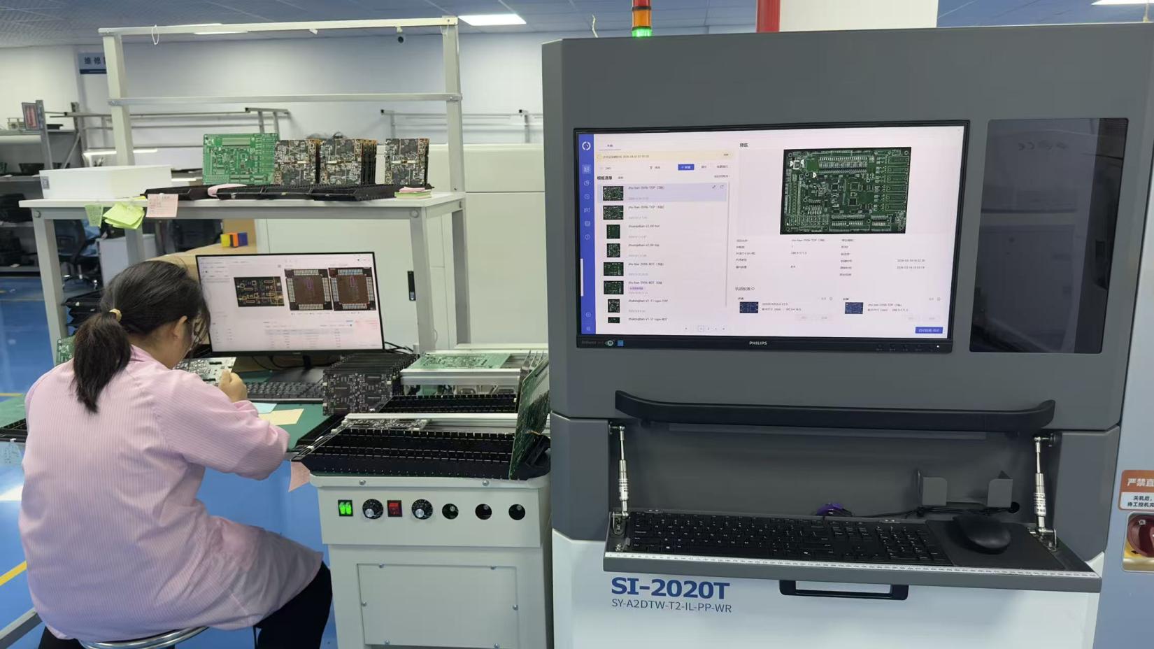
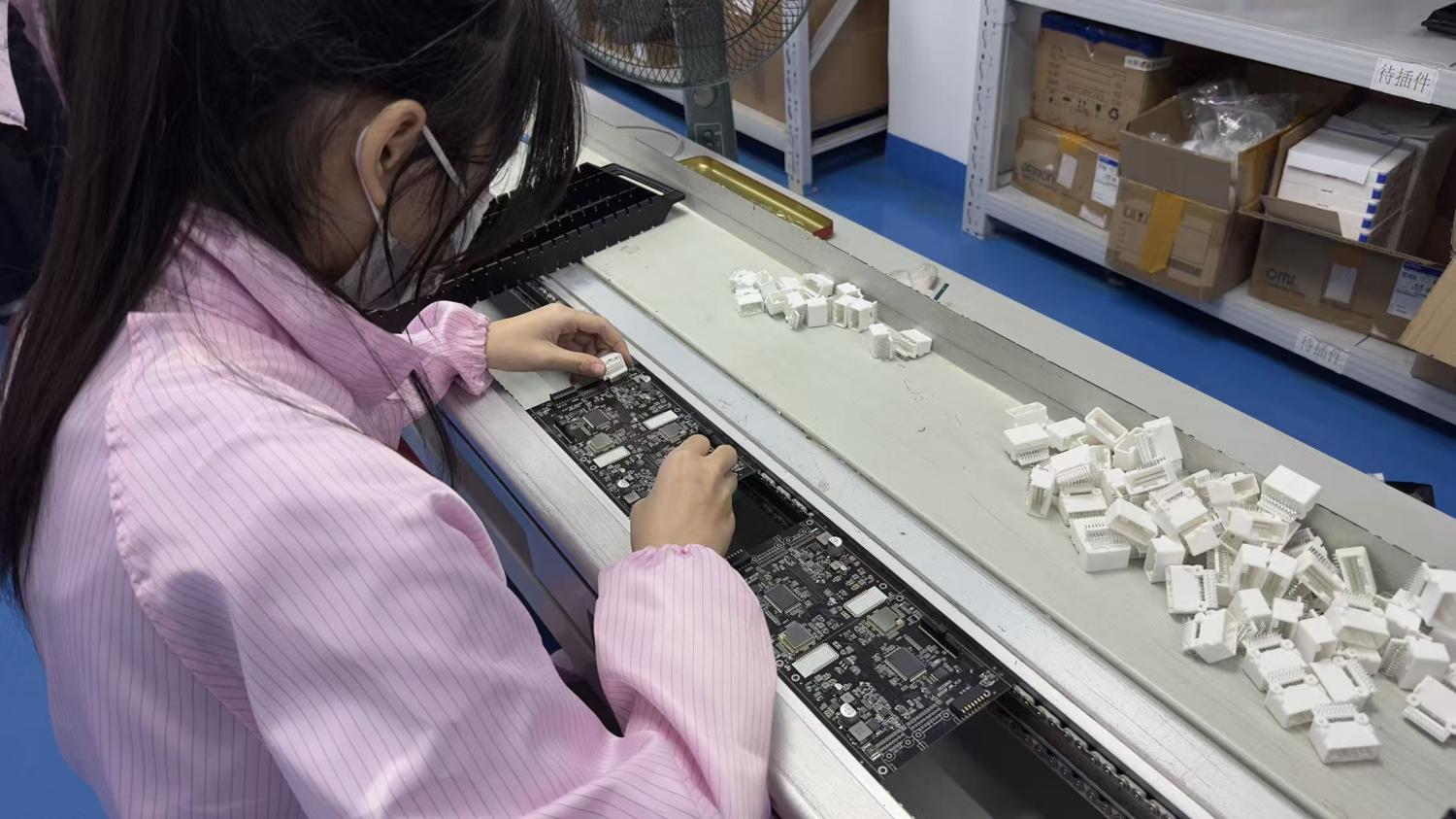
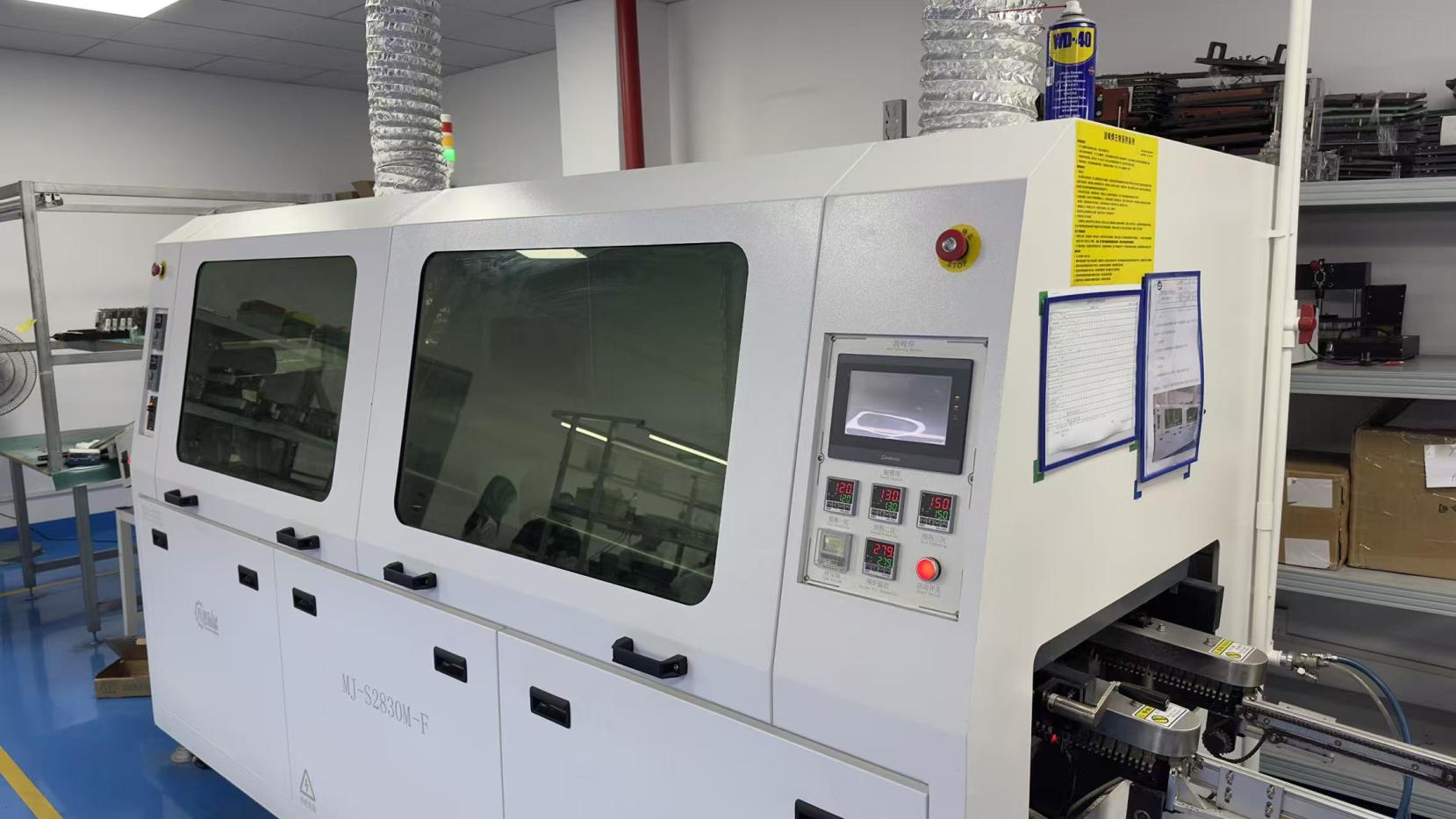
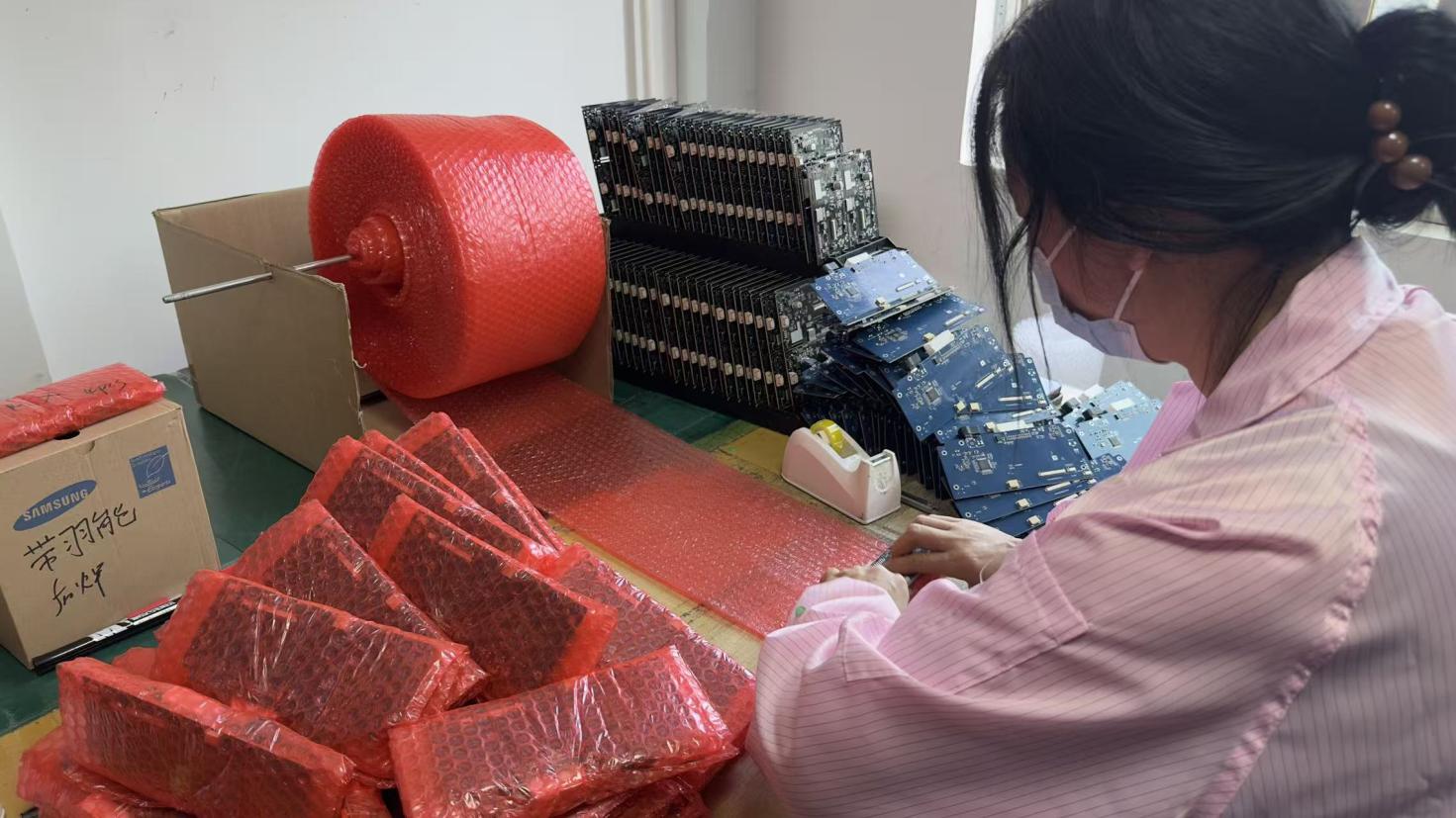
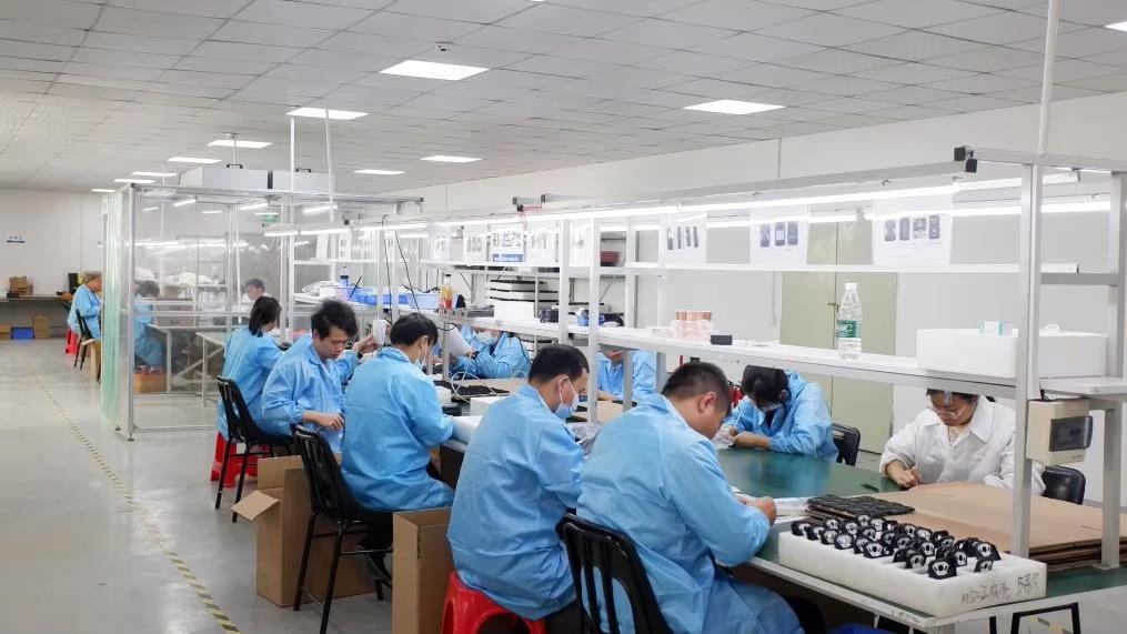
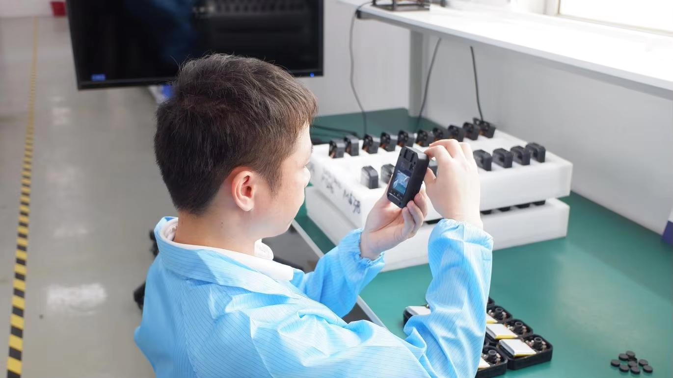
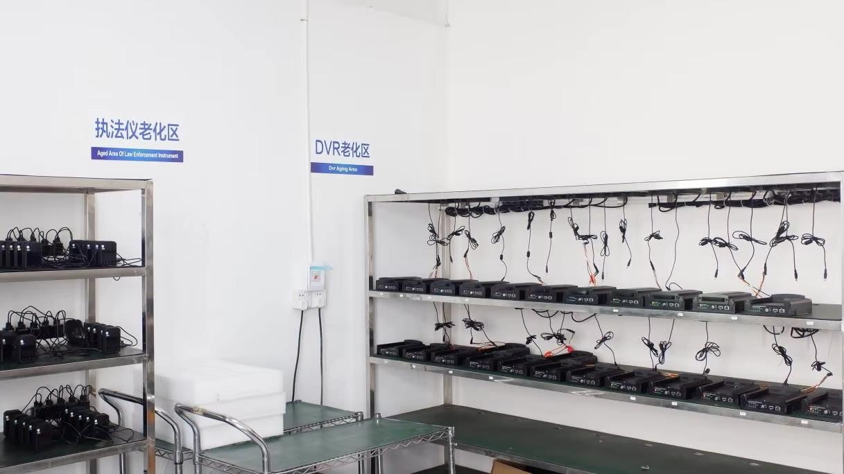
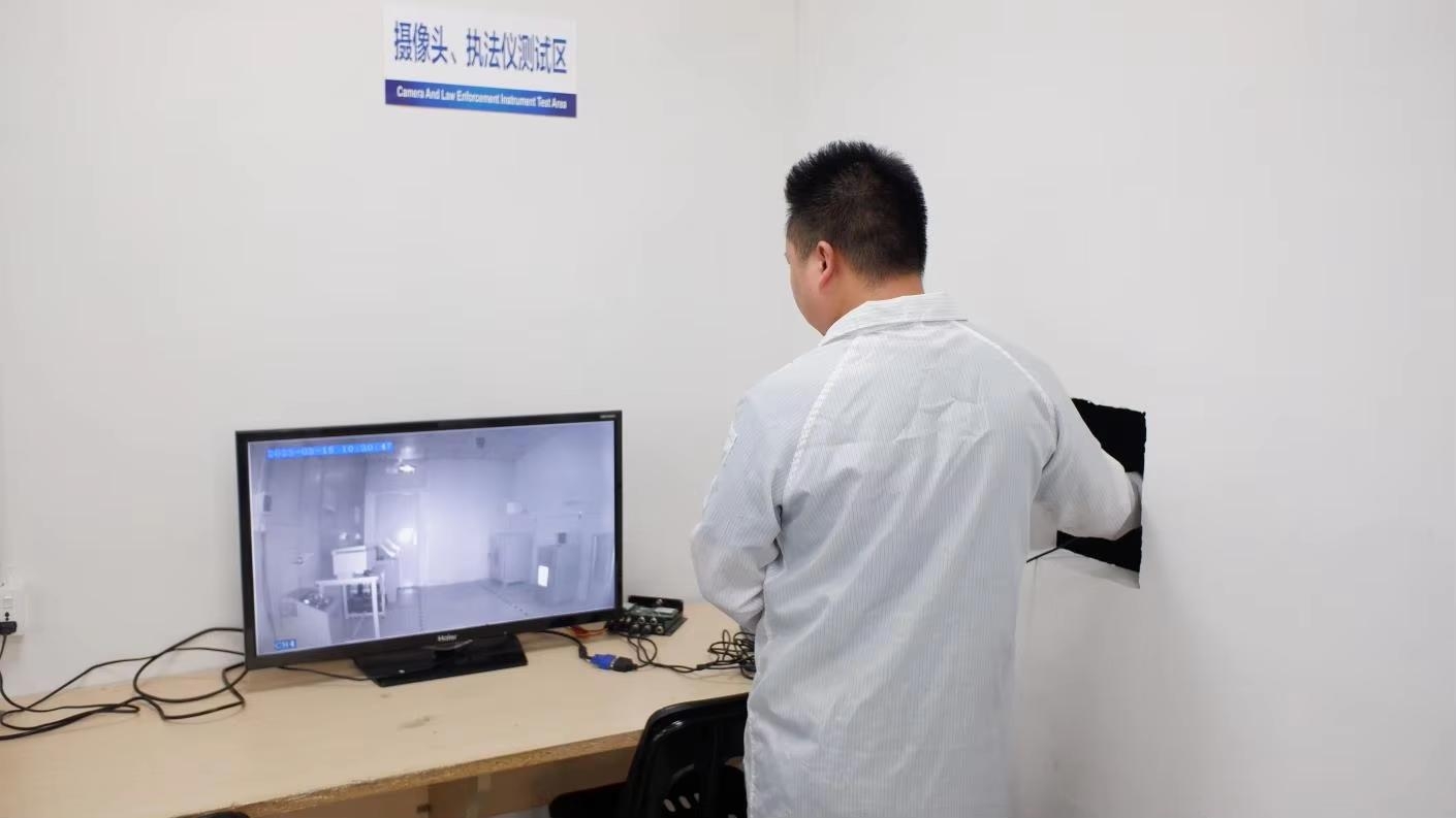

The global thermal imaging market depends on efficient, reliable manufacturing ecosystems to translate physical advancements into affordable laboratory tools. By centralizing our design, sensor manufacturing, wafer packaging, and electronic component assembly within China's premier optoelectronic hub, we optimize every phase of the value chain.
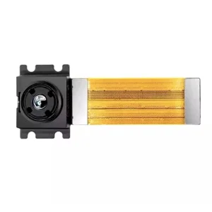
Unlike manufacturers that rely on third-party sensor foundries, our team controls the development process from start to finish. This high level of vertical integration ensures that our raw MEMS wafers, vanadium oxide (VOx) detectors, and germanium optical elements meet strict tolerances. By managing everything internally, we avoid external bottleneck risks and keep our supply chain highly stable.
Moreover, our high production volume enables us to offer professional-grade instruments with spatial resolutions of 640x512 and low NETD values at a lower total cost. This efficiency allows research centers, universities, and industrial laboratories to deploy high-resolution thermographic instruments without stretching their budgets.
When purchasing thermal imaging systems for overseas laboratories, meeting international regulatory standards is critical. Our products conform to major global guidelines, including CE, FCC, and RoHS, ensuring smooth customs clearance and integration into regional research networks.
To simplify deployment, we provide extensive SDK documentation. The included developer toolkits support C++, C#, and Python interfaces, allowing research institutions to integrate our cameras into custom test setups or ROS platforms.
In addition to software support, we provide robust customer service. Our regional service representatives assist with warranty claims, optical recalibration, and hardware maintenance to keep downtime to a minimum.
Scientific thermal cameras serve critical diagnostic roles across several research areas:
The field of scientific thermography is transitioning toward smart, integrated devices:
Dual-Sensor Fusion: Combining LWIR channels with visible-light sensors allows systems to overlay thermal maps onto high-definition photos, helping operators easily identify specific components.
Edge Computing and AI: Modern camera systems run temperature profiling algorithms on the device itself, reducing the need for continuous raw data feeds and external processing.
Lighter, Smaller Cores: The demand for portable thermal cores is rising, leading to the development of USB-powered devices for field and space-constrained applications.
Answers to common technical, commercial, and operational questions from global buyers and research laboratories.
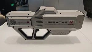
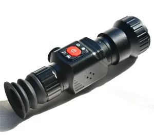
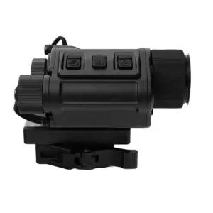
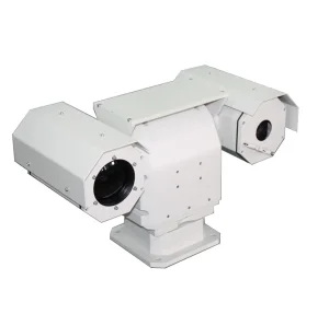
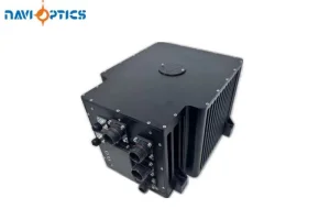
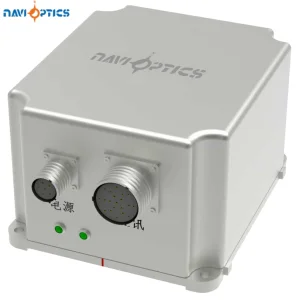
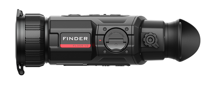
From handheld monoculars to specialized integration cores, explore our complete range of high-precision thermal instruments.